Scientists are developing more highly sensitive devices for the detection of biological and chemical compounds.
Published : Jul 29 , 2016 / DOI : 10.1080/14686996.2016.1202082

Surface plasmon resonance (SPR) devices are the benchmark in optical sensing. They are used for detecting biomarkers of disease, discovering drugs, analyzing chemicals, ensuring food quality and safety, and detecting pollutants in our environment. SPR devices can detect molecules within a few hundred nanometres of their metal surfaces. When a target molecule binds to sensing molecules placed on the device’s surface, this alters the path of light travelling through the medium, changing its “refractive index”. This change of refractive index is used to indicate the molecule’s presence.
—————————————————————————————————————————-
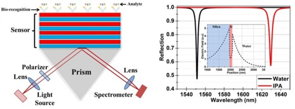
Figure: [left] Sketch of a BSW-based sensor. A bio-recognition layer is attached to the surface to make the sensor selective. Only the desired analytes can attach to the recognition layer resulting in a change in refractive index (n) above the surface. The sensor surface can be separated into arrays of different bio-recognition analytes in order to obtain a multichannel response. [right] Calculated wavelength-dependent reflection in water (n=1.33) and IPA (n=1.37) environments. The inset shows the calculated electric field of fundamental TM mode using a 133 nm-thick silicon layer at an angle of 26.1° with water as the overlying medium.
—————————————————————————————————————————-
Scientists are working on improving the sensitivity, compactness and cost of SPR devices by changing the materials used to make them.
Brian Corbett and Muhammad Khan of University College Cork in Ireland reviewed the latest research in the field of “Bloch surface wave” devices, publishing their findings in the journal Science and Technology of Advanced Materials.
Bloch surface waves (BSW) are light waves that travel on the surface of insulating – or “dielectric” – – alternatively layered materials, shown in the figure. Researchers are testing the use of dielectric materials, instead of the metals typically used for the surfaces of SPR devices, to develop BSW devices. By doing so, they are detecting even smaller changes in the material’s refractive index.
“Bloch surface waves can be used for a variety of sensing applications,” says Corbett. “This research has taken place mainly in the last ten years with demonstrations in sensing vapours, various biomarkers, and protein aggregation, for example. They can also be potentially used as a platform for compact integrated optical circuits,” he says. Corbett expects BSW devices to become commercially available in the coming few years.
Corbett and Khan designed a simple BSW sensor, employing silicon as its surface material, which they believe has practical advantages due to the ease with which it delivers and detects light waves.
“The research shows that surface waves can be easily generated and they provide a sensitive measure to detect the binding of a material at a surface,” says Corbett. “The sensor surface is simple and easy to fabricate with sensitivities comparable and better than SPR sensors. These sensors can provide real-time sensing and may be a way to screen for the presence of biomarkers for different diseases, such as cancer and Alzheimer’s disease, at the doctor’s surgery.”
The sensors still need to be tested for their durability in real environments, says Corbett. The team’s aim is to develop an on-chip sensing platform with high sensitivity that can ultimately be used in bench top or even smartphone-based devices, he says, with potential application in water quality monitoring.
For further information please contact:
Brian Corbett
Tyndall National Institute, University College Cork, Lee Maltings, Cork, Ireland
E-mail: brian.corbett@tyndall.ie
Article information
Brian Corbett and Muhammad Khan: “Bloch surface wave structures for high sensitivity detection and compact waveguiding”, Science and Technology of Advanced Materials Vol. 17 (2016) p. 1202082.
Journal information
Science and Technology of Advanced Materials (STAM) is an international open access journal in materials science. The journal covers a broad spectrum of topics, including synthesis, processing, theoretical analysis and experimental characterization of materials. Emphasis is placed on the interdisciplinary nature of materials science and on issues at the forefront of the field, such as energy and environmental issues, as well as medical and bioengineering applications
For more information about STAM contact
Mikiko Tanifuji
Publishing Director
Science and Technology of Advanced Materials
E-mail: TANIFUJI.Mikiko@nims.go.jp
Information
- Authors
- Muhammad Umar Khan & Brian Corbett
- URL
- https://www.tandfonline.com/doi/full/10.1080/14686996.2016.1202082


